Posts

Showing posts with the label AXI

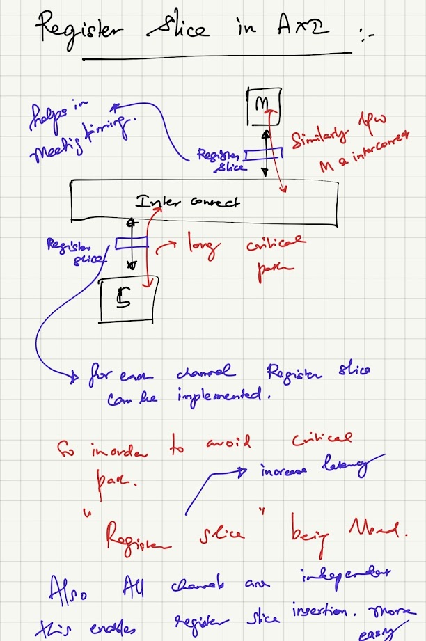
AXI Register Slices

Image

Converting a conventional FIFO into a valid ready based FIFO

Image

AXI4 Lite RTL requirements : Things to keep in mind for Slave implementation

  RTL Requirements : 1. Data width = 32 or 64 bits  (Downsizer may required based on master interface this slave is getting connected with) 2. Burst length supported = 1   ( AxBURST = 0x1 ) 3. Memory type = non-bufferable, non-modifiable (AxCACHE [3:0] = 0x0) 4. Write Strobe = supported 5. Outstanding transaction = Optional to slave Most slave dont support outstanding transaction 6. ID support : Simply slave should reply with ID it been received 7. xLAST = considered as 0x1 for read and write transfer 8. AxLOCK, AxCACHE, AxPROT = 0x0 not supported 9. xRESP - EXOKAY not supported

Introduction to AXI

Image
  Key concepts on how to implement the AXI protocol In older ARM documentation ,  Master and Slave termininology is mentioned.  Now its been changed to Manager and Subordinate.  Advanced Microcontroller Bus Architecture => On chip interconnect specification Benefits of AMBA:  1. IP reuse & Flexibility - Standard interface enables IP reuse across products  2. Compatability - Standard interface helps us in working with different IP vendors  Metrics :  1. Bandwidth  2. Latency AXI is a point to point specification so only interface level info and timing info are concentrated. In order for Multi Manager and Multi Subordinate to be connected. Bus interconnect is required. AXI has 3 channel for write interface and 2 channel for read interface like in above figure.  Why Wr channel has separate response ? Response is required by master which slave acknowledge the transfer is valid for that slave or not . also AW, W are directional from ma...

AXI Outstanding or Active transaction

Image
Active transaction or Outstanding transaction for AXI  Definition of outstanding transaction on Read Channel : Read address is placed and waiting for the read data. Number of such AR transaction accepted between read address and last read data for the particular read address is simply the number of outstanding transaction on read channel Definition of outstanding transaction on Write Channel : For write transactions, the data can come after the address, but leading write data is also allowed. The start of a write transaction can therefore be either of the following: • The transfer of the write address • The transfer of leading write information Therefore, an active write transaction is a transaction for which the write address or leading write data has been transferred, but the write response has not yet been transferred. Simply we can say the number of transaction accepted on AW channel between first AW and the Bresp on the write channel will give outstanding transaction on w...

Basic Memory Mapping in SoC

Image
Memory map or Address map gives information regarding how much address locations that a processor can access. The memory map shown below is taken from the ARM principles of Memory map whitepaper. Figure 1 shows a memory map or an address map organization for a typical SoC. Figure 1: 32-bit memory map  Figure 2: Versatile version of the 32bit ARM CPU Memory map Address map consists of Boot ROM: This Boot ROM address region for ARM CPU 32bit to start from 0x0000_0000 or 0xFFFF_0000 ROM, RAM, SoC I/O: This address region is recommended to align with 64KB and consists of Internal ROM, SRAM, static memory, SoC peripheral registers  Mapped I/O and additional SoC I/O: Address region of mapped I/O like PCIe DRAM address space: The address space recommended for DRAM should be contiguous and needs to  be placed near the high address region  of the memory map   Reference: [1] Principles of ARM Memory Maps [White Paper] http://infocenter.arm.co...